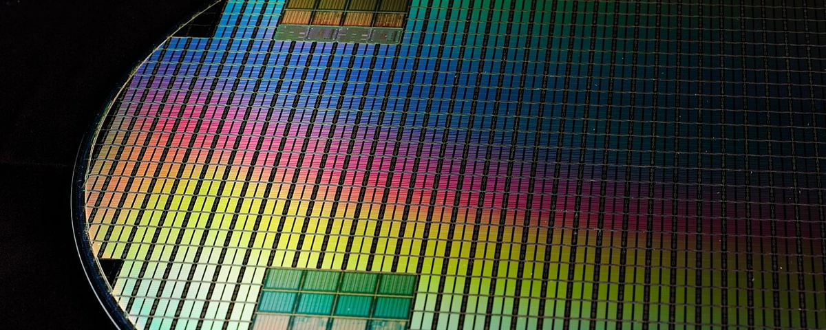
The transistor made an excellent replacement for the vacuum tube. It was smaller, needed no glowing cathode, and could perform its electrical duties without first being brought up to cooking temperature. For an industry that had recently considered a room full of hot glass a reasonable arrangement for doing arithmetic, these were substantial improvements.
But a transistor was still a component. It had to be manufactured, handled, connected to other components, and persuaded to cooperate with them. Replace a vacuum tube with a transistor and the switch became smaller. The circuit surrounding it did not automatically follow.
By the late 1950s, electronics was accumulating the consequences of its own success. More ambitious machines required more parts. Every additional part brought connections, assembly work, and opportunities for error. Engineers could draw increasingly elaborate circuits, but somewhere those drawings had to become objects. The pencil was having a much easier time of it than the factory.
Consider an ordinary electrical connection. On a diagram, it is a line. It costs almost nothing to draw and can be lengthened, shortened, or moved with a rubber eraser. In a machine, that line must become conducting material, attached at both ends and kept from touching whatever it should not touch. Somebody must make it, inspect it, and provide space for it. Repeat this often enough and the lines begin competing with the components for possession of the machine.
Making the transistor smaller helped, but it also made the surrounding arrangement look increasingly unreasonable. The useful electrical action occurred inside a tiny region of semiconductor. Much of the visible apparatus existed to connect that region to another one.
The next opportunity lay in the space between the parts.
At Texas Instruments, Jack Kilby approached the problem by questioning why the parts had to begin their lives separately. A transistor required semiconductor material. Could the same material also provide the other electrical functions a circuit needed? Resistance could come from a suitably shaped region through which current had difficulty passing. Capacitance could come from structures that stored separated electrical charge. Perhaps the factory did not need to manufacture a collection of different objects and introduce them afterward.
On September 12, 1958, Kilby demonstrated an oscillator assembled from transistor, resistor, and capacitor elements fashioned from germanium. Fine gold wires connected the elements. The device produced an electrical oscillation, a repeating signal that established that the arrangement worked. It was a small demonstration of a large proposition: semiconductor material could supply an entire circuit’s functions. The wires, however, remained awkward companions. They were adequate for proving an idea and poorly suited to manufacturing it in quantity. Computer History Museum: Kilby’s solid circuit
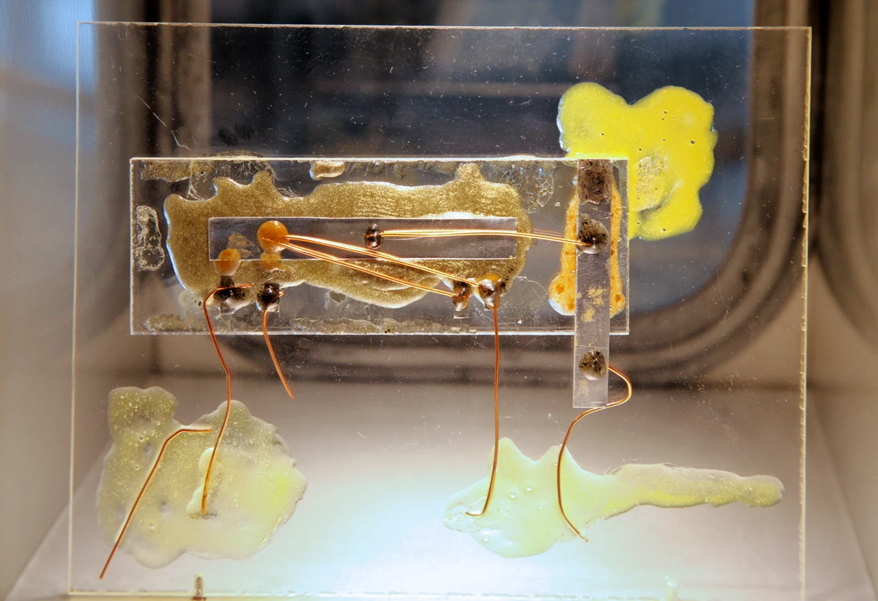
An oscillator was a sensible place to begin. Its output repeated, so its operation could be observed directly. Kilby did not need to build a computer to demonstrate the principle, any more than someone inventing a better brick needs to begin with a cathedral.
The unanswered question was how to turn the demonstration into a manufacturing method. If each little circuit still required delicate wires to be attached individually, the industry would have made its assembly problem smaller without making it much less troublesome.
In California, a different difficulty was producing a useful answer.
Fairchild Semiconductor was learning how to manufacture silicon transistors reliably. Silicon had electrical advantages, but its exposed surface could be an uncooperative place. A transistor depends on carefully controlled boundaries between regions with different electrical properties. Disturb those boundaries and current may leak where it should not, or the device may behave differently from the one beside it.
Jean Hoerni proposed leaving a protective layer of silicon dioxide over the sensitive junctions. Earlier manufacturing methods used oxide as a temporary aid and then removed it. Hoerni saw a reason to let it stay. He recorded the idea in December 1957 and demonstrated a working transistor using the approach in March 1959. The resulting method became known as the planar process. It protected the device while allowing its important structures to be manufactured from the wafer’s upper surface. Computer History Museum: the planar process
The practical value of protection was becoming painfully clear. In 1959, Gordon Moore investigated failures in Fairchild transistors supplied to an aerospace customer. Tapping the packages caused some devices to fail. Inside, loose material could move across exposed junctions and create unwanted electrical connections. For a time, the company tested devices by striking their packages to find troublesome units before shipment.
This is the sort of activity generally omitted from diagrams showing the triumphant advance of technology. Nevertheless, it was useful work. A transistor that failed when tapped was better discovered at the factory than inside its customer’s equipment.
The surviving notebooks also complicate the convenient version of the story. Hoerni had resumed serious work on his protective process before Moore identified the loose-particle problem. The process helped solve it, but the dates do not support treating that particular failure as the original inspiration. The inventions were finding uses as the problems became understood. Computer History Museum: the Fairchild notebooks
Robert Noyce recognized that Hoerni’s oxide layer could serve another purpose. Silicon dioxide was an electrical insulator. Metal connections could run across its surface without making unwanted contact with the silicon underneath. Open a small window where a connection was required, let the metal reach the appropriate device, and keep it insulated everywhere else.
The connections could become part of the manufacturing process.
Noyce’s 1959 patent described an arrangement in which devices formed within silicon were joined by metal deposited over the protective oxide. This provided a practical route to a complete circuit on one chip. Kilby and Noyce are consequently recognized as co-inventors of the integrated circuit, although their contributions addressed different parts of the problem. Kilby demonstrated the possibility of an all-semiconductor circuit. Noyce supplied the metal-over-oxide interconnection scheme that made a manufacturable monolithic structure possible. Computer History Museum: Noyce’s integrated-circuit concept
The wires had not literally vanished. Electricity still needed conducting paths. What changed was how those paths came into existence. Instead of installing each connection as a separate object, manufacturers could form many connections together as a pattern.
That distinction sounds modest until one considers repetition. A worker assembling a circuit must repeat the work for the next circuit. A manufacturing pattern can be reproduced. Improving the process then improves the production of every circuit that uses it.
There was still considerable distance between Noyce’s proposal and a dependable product. Jay Last led the Fairchild team that undertook the work. One difficulty was keeping neighboring components electrically separate inside a shared piece of semiconductor. Putting devices close together was useful only if current continued to obey the intended circuit.
The team’s first working monolithic devices, produced in May 1960, used deep channels etched into the silicon and filled with insulating epoxy. A later version achieved isolation electrically, using appropriately arranged semiconductor junctions. Working circuits using that production approach followed in September. The achievement belonged to a team solving fabrication, isolation, and circuit-design problems together, including Isy Haas, Lionel Kattner, Robert Norman, and others. Computer History Museum: the first planar integrated circuits
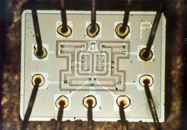
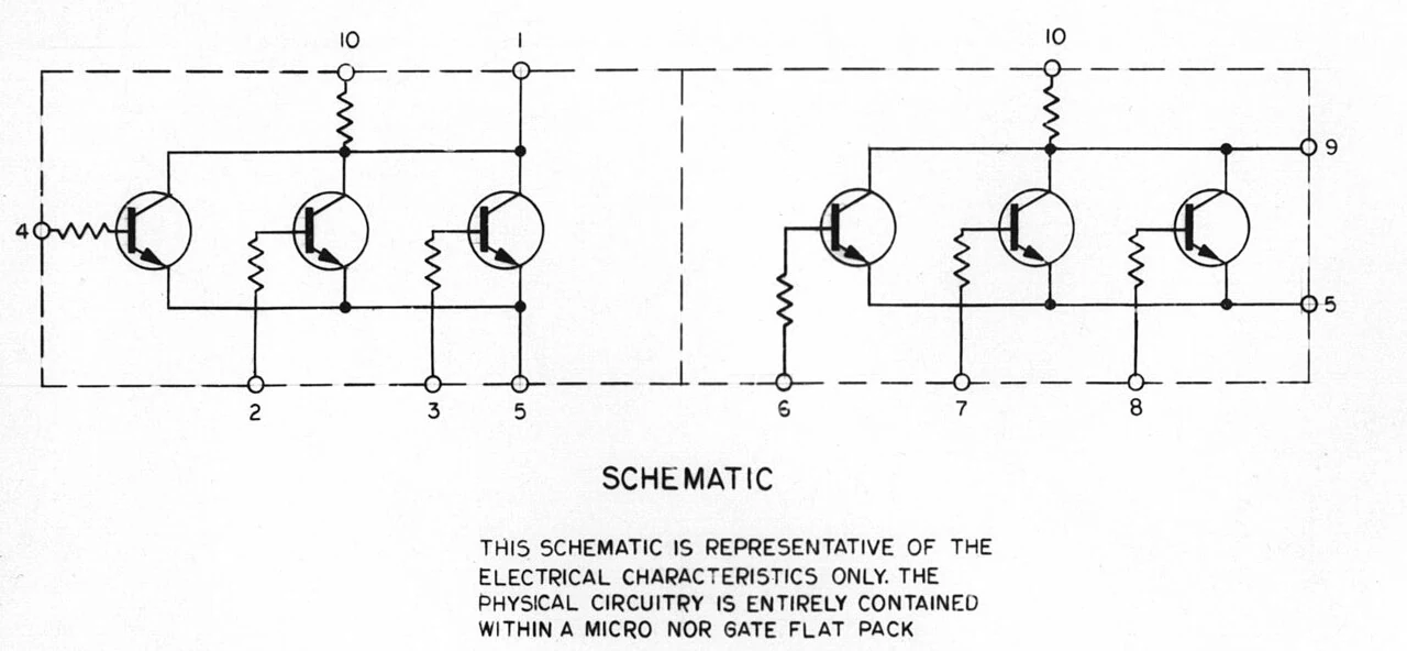
The semiconductor industry was beginning to adopt a peculiar form of construction. Instead of picking up small objects and putting them where they belonged, it would alter selected regions of a surface until the necessary structures existed there.
Photography helped make this possible.
During the 1950s, researchers adapted photoengraving techniques to semiconductor production. A light-sensitive coating covered the wafer. Light passed through a patterned mask, changing selected parts of the coating. Developing the coating and etching the material underneath opened precisely located windows. Through those windows, manufacturers could introduce impurities that changed the silicon’s electrical behavior.
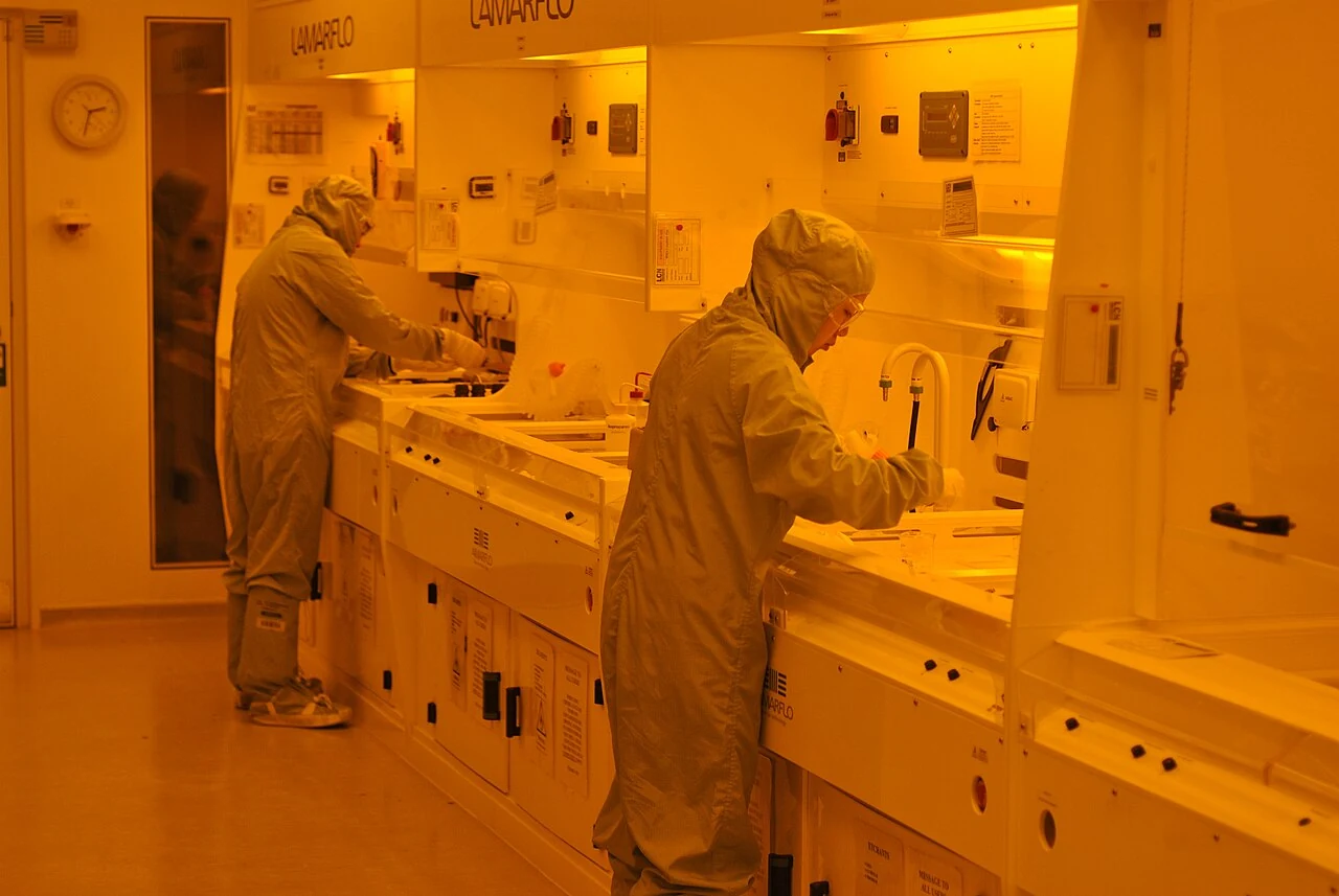
The apparently undesirable word impurity concealed an essential distinction. An unwanted contaminant could spoil a device. A carefully chosen element, introduced in a controlled amount at the correct location, could help create one. Semiconductor manufacturing required exceptional cleanliness so that the factory could decide which impurities were permitted.
By 1958, Last and Noyce were building equipment at Fairchild to repeat photographic patterns across a wafer. The same slice could carry many devices through shared processing steps. Computer History Museum: early semiconductor photolithography
A chip therefore emerges through a sequence of transformations. Materials are added. Selected areas are protected. Other areas are exposed and removed. Electrical properties are altered. Conducting paths are formed and separated by insulating layers. Patterns must line up with earlier patterns, because a connection that arrives near its destination has not necessarily arrived at its destination.
Modern factories perform far more elaborate versions of these operations, but the underlying method remains recognizable. A polished wafer passes through repeated processing steps before it is divided into individual chips, which are tested and packaged for use. The circuit is built into and above the semiconductor through controlled changes to material. ASML: semiconductor manufacturing steps
This did not make manufacturing easy. It changed which difficulties mattered.
Imagine a wafer intended to produce 100 identical chips. If only 10 work, the successful chips must carry the expense of processing the other 90. Improving the proportion that works can lower the cost without changing the circuit’s design at all. Conversely, an ingenious circuit that rarely survives fabrication may be an impressive way to lose money.
The useful measure is called yield: the share of manufactured devices that meet the required standard. It gives cleanliness, repeatability, and process control an immediate economic significance. A defect may be microscopic; its consequences appear at full size in the accounts.
The new method also changed where human effort was spent. Far more work could go into designing the circuit and perfecting its production process before a customer received anything. Once those tasks succeeded, the same design could be reproduced without repeating every act of assembly by hand. The factory became more complicated so that the individual product could become simpler to make.
Finding customers willing to support that development was another matter.
Early integrated circuits were expensive, performed limited functions, and did not automatically outperform familiar alternatives. A company building equipment for an office could reasonably ask why it should pay more for a new component that replaced only a few inexpensive old ones.
A spacecraft offered a different calculation.
Size, weight, and power consumption had unusual value when the entire machine had to be launched. Military and aerospace programs became important early customers, including Apollo and Minuteman. The Apollo Guidance Computer, designed at MIT and manufactured by Raytheon, helped establish a substantial market for integrated logic circuits. Such programs bought devices while the technology was still costly and demanding, giving manufacturers both orders and stringent requirements to meet. Computer History Museum: early aerospace applications
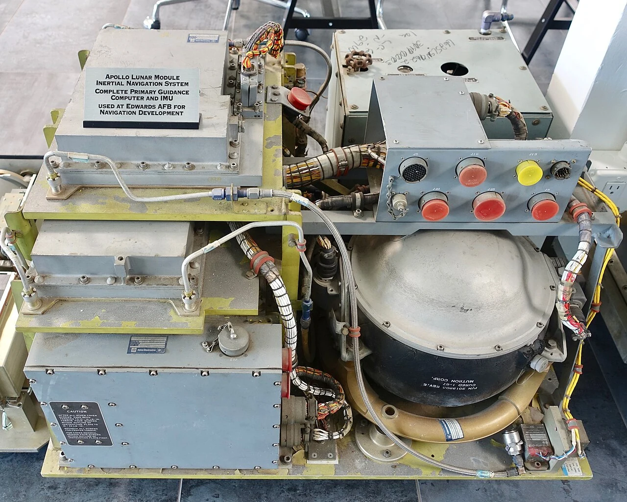
These customers did not make the chips affordable by wishing to go somewhere impressive. Their orders supported production, testing, and refinement. They gave an immature manufacturing process the opportunity to become an experienced one.
Meanwhile, another transistor was arriving with characteristics particularly suited to integration.
At Bell Labs, Mohamed Atalla and Dawon Kahng developed a successful insulated-gate field-effect transistor in 1959 and demonstrated it in 1960. A voltage applied to a gate could influence the conducting region beneath it, despite an insulating oxide layer separating the two. The electric field controlled the availability of mobile charge in the semiconductor and therefore how readily current could pass.
The arrangement became known as the MOS transistor, from its metal, oxide, and semiconductor structure. Its early performance did not make it an obvious winner for the telephone system. Yet its potential for compact fabrication attracted researchers elsewhere. An initially unexciting device could become valuable when the question changed from how well one transistor performed to how effectively many could be manufactured together. Computer History Museum: the MOS transistor
This was an important change in judgment. The best individual component was not necessarily the component that produced the best large system. Manufacturing convenience, density, power, and cost could matter as much as the speed of one isolated device.
Gordon Moore was watching the economics closely. In 1965, he described a striking trend: the number of components in an integrated circuit at the most economical cost per component had been increasing rapidly. His projection suggested approximately annual doubling over the following decade. In 1975, he revised the expected future pace to roughly a doubling every two years. Computer History Museum: Moore’s original forecast
The forecast eventually acquired the status and name of a law, which can make the underlying work sound rather more automatic than it was. A calendar could announce that another year had passed. It could not improve a chemical process, align a mask, remove a defect, or design a better transistor.
Nor did doubling components promise that every computer program would finish twice as quickly. Moore was describing an extraordinary progression in what manufacturers could economically put on a chip. What designers and programmers could do with those components was a related but separate question.
Before long, the available space and fabrication techniques permitted a more ambitious kind of integration. Instead of placing a few logic functions on a chip, engineers could attempt the central processing functions of a computer.
Intel’s 4004, introduced in 1971, contained about 2,300 transistors. Ted Hoff and Stanley Mazor contributed its architectural conception; Federico Faggin led its realization in silicon, assisted by Masatoshi Shima. It still required supporting chips to make a complete system, but the central processor had become a component that another designer could buy. Computer History Museum: the microprocessor
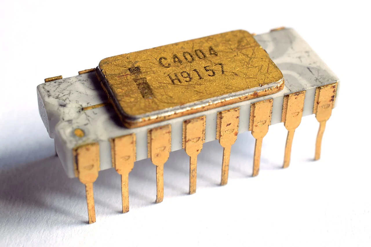
That development altered the entrance requirements for computing. A manufacturer no longer had to begin by designing an entire processor from individual logic components. It could incorporate one, connect memory and suitable inputs and outputs, and concentrate on the task its product needed to perform.
Computation could move into objects that would never have justified a dedicated computer room. The economic question shifted from whether an organization could afford a computer to whether a particular product could benefit from having some computing inside it. Eventually, the answer would include enough ordinary objects that people stopped finding the arrangement remarkable.
The integrated circuit had made this expansion possible by changing the relationship between complexity and assembly. More electronic capability no longer required a proportionate increase in separately handled parts. A factory could reproduce a dense arrangement of devices and connections that would have been hopelessly laborious to assemble individually.
But the resulting abundance exposed another difficulty.
A calculation is more than a collection of switches. It has an order. Some operations can proceed independently; others need the result of an earlier operation before they can begin. Put more arithmetic hardware beside a strictly dependent sequence and the additional hardware may have nothing useful to do.
Gene Amdahl had already examined the limits this imposed on parallel computing in 1967. The portion of a task that must remain sequential constrains how much faster the whole task can become when other portions are spread across additional processors. More machinery cannot remove a dependency merely by standing nearby. Amdahl’s original paper
As fabrication supplied more transistors, computer designers gained room to try increasingly elaborate arrangements. They could store more information close to the arithmetic, anticipate upcoming work, overlap operations, or provide additional processing units. Each choice helped particular kinds of work and consumed some of the available space and power.
The factory had learned how to provide an extraordinary number of switches. The next challenge was organizing them so that the problem at hand could actually use them.
A long calculation with tightly dependent steps wanted one kind of machine. A vast collection of similar calculations, many of which could proceed together, offered a different opportunity. The distinction would eventually send computing toward hardware that had been learning how to draw pictures.
The circuit had disappeared into silicon. What remained stubbornly visible was the time required to finish the work.
Sources and further reading
- Computer History Museum: Kilby’s solid circuit
- Computer History Museum: the planar process
- Computer History Museum: the Fairchild notebooks
- Computer History Museum: Noyce’s integrated-circuit concept
- Computer History Museum: the first planar integrated circuits
- Computer History Museum: early semiconductor photolithography
- ASML: semiconductor manufacturing steps
- Computer History Museum: early aerospace applications
- Computer History Museum: the MOS transistor
- Computer History Museum: Moore’s original forecast
- Computer History Museum: the microprocessor
- Amdahl’s original paper